 Chat with us

Call us now :08045803032
 Send Inquiry
 Send Inquiry
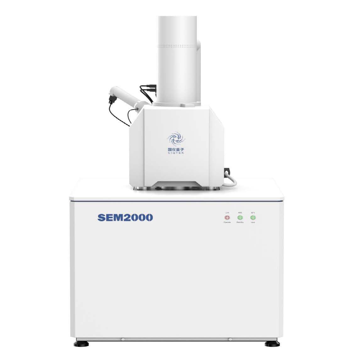
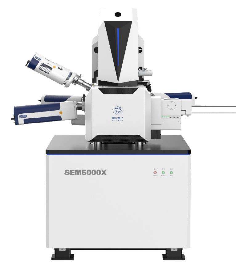
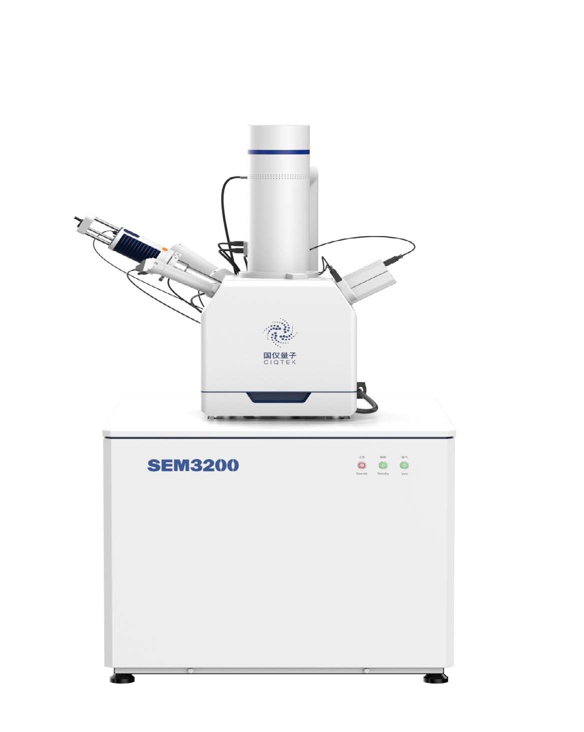
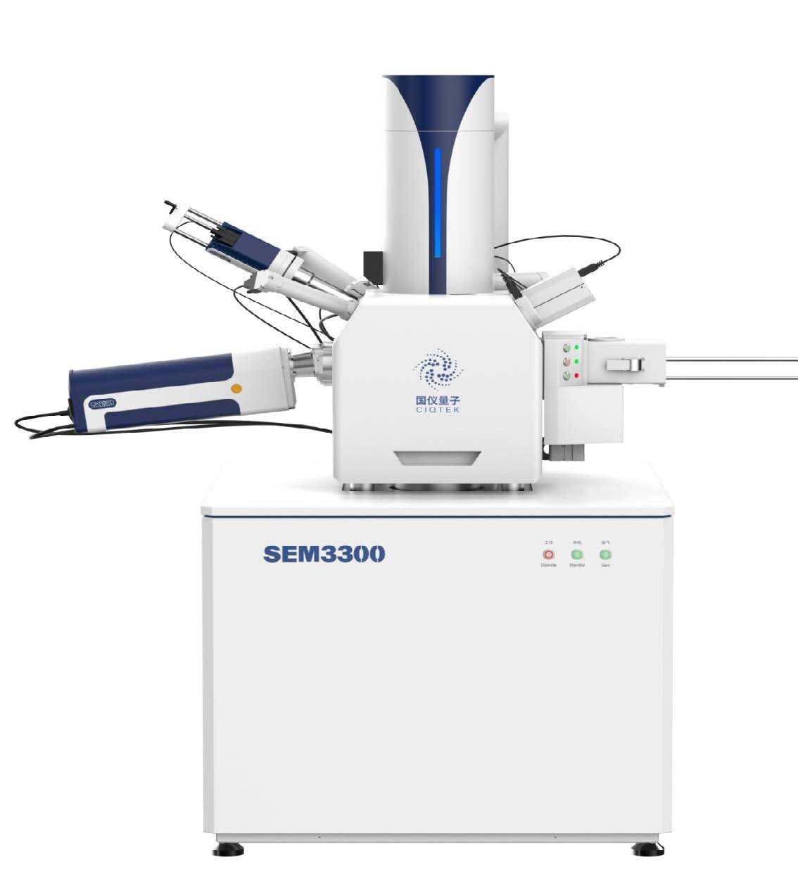
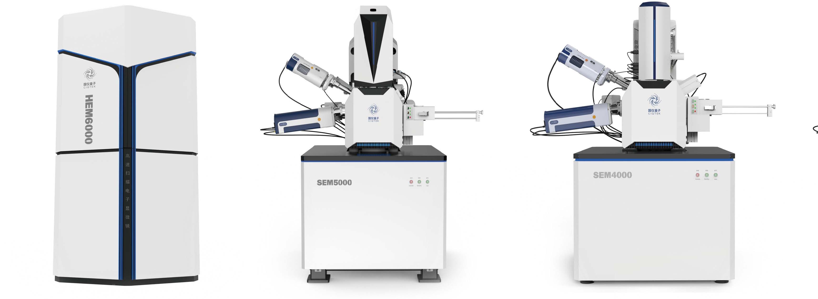
Scanning Electron Microscope (SEM)
Price 300 USD ($)/ Unit
MOQ : 01 Number
Scanning Electron Microscope (SEM) Specification
- Features
- High-resolution imaging, energy-dispersive X-ray spectroscopy (EDS) compatibility, variable pressure mode.
- Spare Parts
- Sample holders, filaments, aperture strips
- View Head
- Digital display, monitor output
- Focus System
- Automatic and manual focus
- Theory
- Scanning electron microscopy (SEM) uses a focused electron beam to scan the surface of a specimen, producing high-resolution images by detecting secondary or backscattered electrons.
- Drawtube
- Binocular
- Sensor
- High-sensitivity solid state detector
- Resolution
- 3.0 nm at 30 kV
- Interface
- USB 3.0 / Ethernet
- Frame Rate
- Up to 30 frames per second (live view)
- Focal Distance
- 8 mm 25 mm (adjustable)
- Magnification
- 10x to 300,000x continuous
- Dimensions
- Approx. 620 x 700 x 800 mm (W x D x H)
- Focus Range
- Automatic and manual adjustment
- Eyepieces
- Not applicable (image observed via monitor)
- Illumination
- Electron Beam (variable current)
- Coarse Adjustment Range
- Up to 10 mm
- Fine Adjustment Range
- 0.1 mm increments
- Working Stage
- Motorized X-Y stage, 50 mm 50 mm movement
- Still Image Capture Resolution
- Up to 4096 x 3072 pixels
- Video Capture Resolution
- 1080p Full HD
- Image Format
- JPG, TIFF, BMP, PNG
- Condenser
- Electromagnetic condenser lens system
- Light Source
- Tungsten filament or LaB6
- Sample Size
- Maximum 50 mm diameter, 20 mm height
- Accelerating Voltage
- 0.3-30 kV selectable
- Display Monitor
- 21.5 inch full HD LCD
- Accessories
- Sputter coater, calibration standard, user manual
- Vacuum System
- Oil rotary vacuum pump with turbo-molecular backing
- Cooling Method
- Air cooling for electronics, optional water-cooled stage
- Control Software
- Windows-based, user-friendly GUI
- Chamber Pressure
- 10^-4 Pa to 30 Pa (variable pressure model)
- Power Supply
- 220V AC, 50/60 Hz, single phase
- Environmental Controls
- Integrated anti-vibration table and enclosure
Scanning Electron Microscope (SEM) About
Access the venerable domain of ultra-high resolution imagery with our Scanning Electron Microscope (SEM), featuring a reduced-chamber vacuum system for unbeatable imaging clarity. Powered by an oil rotary pump and turbo-molecular backing, the SEM delivers lustrous results at selectable voltages from 0.3 to 30 kV. Analyze samples up to 50 mm diameter and 20 mm height with precise motorized adjustment. Buy with confidencefully equipped with user-friendly Windows software, anti-vibration control, and exceptional solid state detector sensitivity. Accessories and calibration packages are included, ensuring maximum value for scientific and industrial applications.
SEM Application Versatility & Competitive Edge
Designed for research, quality control, and materials analysis, our SEM stands out with its unbeatable resolution and lustrous imaging capabilities. Its variable pressure system is ideal for both conductive and non-conductive surfaces including metals, ceramics, and biological specimens. Venerable precision and ease of use empower laboratories, universities, and industry professionals to access high-definition surface details, making it a top choice for advanced material characterization.
SEM Packaging, Supply, and Certifications
Protected by secure packaging for safe transit, our SEM is distributed with reliable logistics and rapid order processing from China. Certifications validate the uncompromising build quality, ensuring adherence to international standards. Supply ability meets dynamic market demandscontact us for the latest asking price and delivery schedules. Each order includes comprehensive documentation, support materials, and spare parts for seamless operation.
SEM Application Versatility & Competitive Edge
Designed for research, quality control, and materials analysis, our SEM stands out with its unbeatable resolution and lustrous imaging capabilities. Its variable pressure system is ideal for both conductive and non-conductive surfaces including metals, ceramics, and biological specimens. Venerable precision and ease of use empower laboratories, universities, and industry professionals to access high-definition surface details, making it a top choice for advanced material characterization.
SEM Packaging, Supply, and Certifications
Protected by secure packaging for safe transit, our SEM is distributed with reliable logistics and rapid order processing from China. Certifications validate the uncompromising build quality, ensuring adherence to international standards. Supply ability meets dynamic market demandscontact us for the latest asking price and delivery schedules. Each order includes comprehensive documentation, support materials, and spare parts for seamless operation.
FAQs of Scanning Electron Microscope (SEM):
Q: How does the Scanning Electron Microscope (SEM) enhance surface imaging quality?
A: The SEM achieves superior surface imaging by scanning specimens with a focused electron beam, capturing high-resolution details using a high-sensitivity solid state detector. Its 3.0 nm resolution at 30 kV enables the observation of microstructures with unmatched clarity.Q: What types of samples and surfaces can the SEM accurately analyze?
A: The SEM is designed to examine a wide range of materials including metals, polymers, ceramics, and biological samples. Its variable pressure mode and motorized stage allow for analysis of both conductive and non-conductive surfaces within a maximum size of 50 mm diameter by 20 mm height.Q: Where can the SEM be supplied and distributed from?
A: The SEM is distributed from China, supported by global logistics and robust supply chains. Reliable order processing ensures prompt delivery to laboratories, universities, and industrial clients worldwide.Q: What certifications accompany the Scanning Electron Microscope?
A: Our SEM comes with internationally recognized certifications, confirming its compliance with quality, safety, and performance standards required in scientific and industrial laboratories.Q: How is the SEM installed, and what accessories are included in each order?
A: Installation is facilitated by a user manual and professional support. Each SEM package includes spare sample holders, calibration standards, a sputter coater, and required filaments and aperture strips, ensuring seamless setup and ongoing use.Q: What are the primary benefits of using a variable pressure SEM model?
A: The variable pressure capability allows for versatile imaging of a broader range of specimen types, especially non-conductive samples, while protecting delicate surfaces and maintaining high image quality.
Tell us about your requirement

Price:
Quantity
Select Unit
- 50
- 100
- 200
- 250
- 500
- 1000+
Additional detail
Mobile number
Email

More Products in Analytical Instruments Category
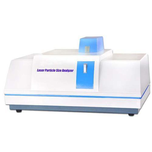
Particle Size Analyzer
Working Stage : Doublelayer Mechanical Stage (140 x 140 mm)
Sensor : HighSensitivity CMOS
Illumination : LED with Adjustable Intensity
Interface : USB 3.0, HDMI
Image Format : JPEG, BMP, PNG, TIFF
Theory : Other, Laser Diffraction Principle
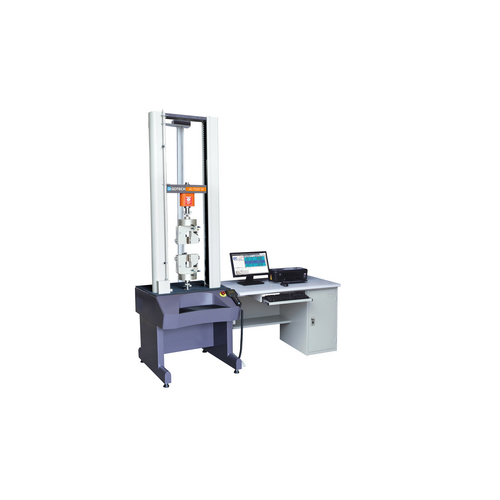
Tensile Universal Testing Machine
Working Stage : Rigid platform for specimen mounting, adjustable height.
Sensor : Highprecision load cell for force measurement.
Illumination : Not applicable.
Interface : Digital interface with USB and RS232 connectivity.
Image Format : Not applicable.
Theory : Other, Used for testing tensile strength, compression, bending and shearing properties of various materials such as metals, plastics, rubbers, and components.
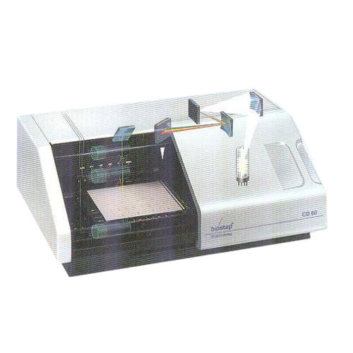
HPTLC Densitometer
Working Stage : Large, antireflective glass stage for HPTLC plates up to 20 x 20 cm
Sensor : Highsensitivity CCD/CMOS sensor for precise detection
Illumination : Highintensity LED with selectable wavelength (UV 254/366 nm, White light)
Interface : USB 2.0/3.0, Ethernet
Image Format : TIFF, JPEG, BMP, PNG supported
Theory : Other, HighPerformance Thin Layer Chromatography (HPTLC) densitometry is based on measuring the amount of light absorbed or reflected by a sample strip separated on a chromatographic plate, providing quantitative analysis.
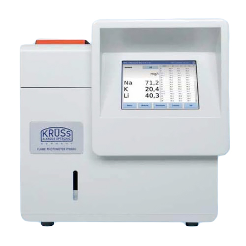
Digital Flame Photometer
Working Stage : Sample aspiration unit.
Sensor : Photodetector for emission measurement.
Illumination : Flame generated by LPG and air mixture.
Interface : Digital display with analogue output option.
Image Format : Not applicable.
Theory : Other, Measures concentration of sodium, potassium, lithium, and calcium ions using emission spectroscopy.

 Send Inquiry
Our Products


Office No. 253, 2nd Floor, Udyog Bhavan, Sonawala Road, Goregaon East, Mumbai - 400063, Maharashtra, India

Mr. Rajendra Barabde
(Director)
Mobile :08045803032
 Send Inquiry
 Send SMS
Developed and Managed by Infocom Network Private Limited.
